7489 IC wiring | pin diagram |Replacing 74189 or 74219 with 7489 IC: Working, Wiring, and Differences Explained
Contents
Learn how to use 7489 RAM IC , including its complete pinout.Differences from similar chips like the 74189. Understand its open-collector outputs, how to wire it properly with DIP switches and a push button for write control, and build your own interactive RAM module."
If you're struggling to find the 74189 or 74219 ICs in the market, you're not alone—these memory chips have become increasingly rare and difficult to source. Fortunately, the 7489 IC is still widely available and can be used as a suitable replacement in many applications
Whether you're following a RAM-building tutorial by Ben Eater or working on your own project and got stuck due to unavailable ICs, the 7489 offers a practical alternative. However, understanding its differences, wiring requirements, and behavior compared to the 74189 or 74219 is essential for a successful substitution.
Lets go ..
What Are These ICs?
74189 or 74LS189 and 74219 or 74LS219 are 64-bit (16×4) RAM ICs used in older digital systems.
7489 is also a 64-bit (16×4) RAM IC, but it differs slightly in pinout and read/write behavior.
Detailed pinout diagram of 7489 IC
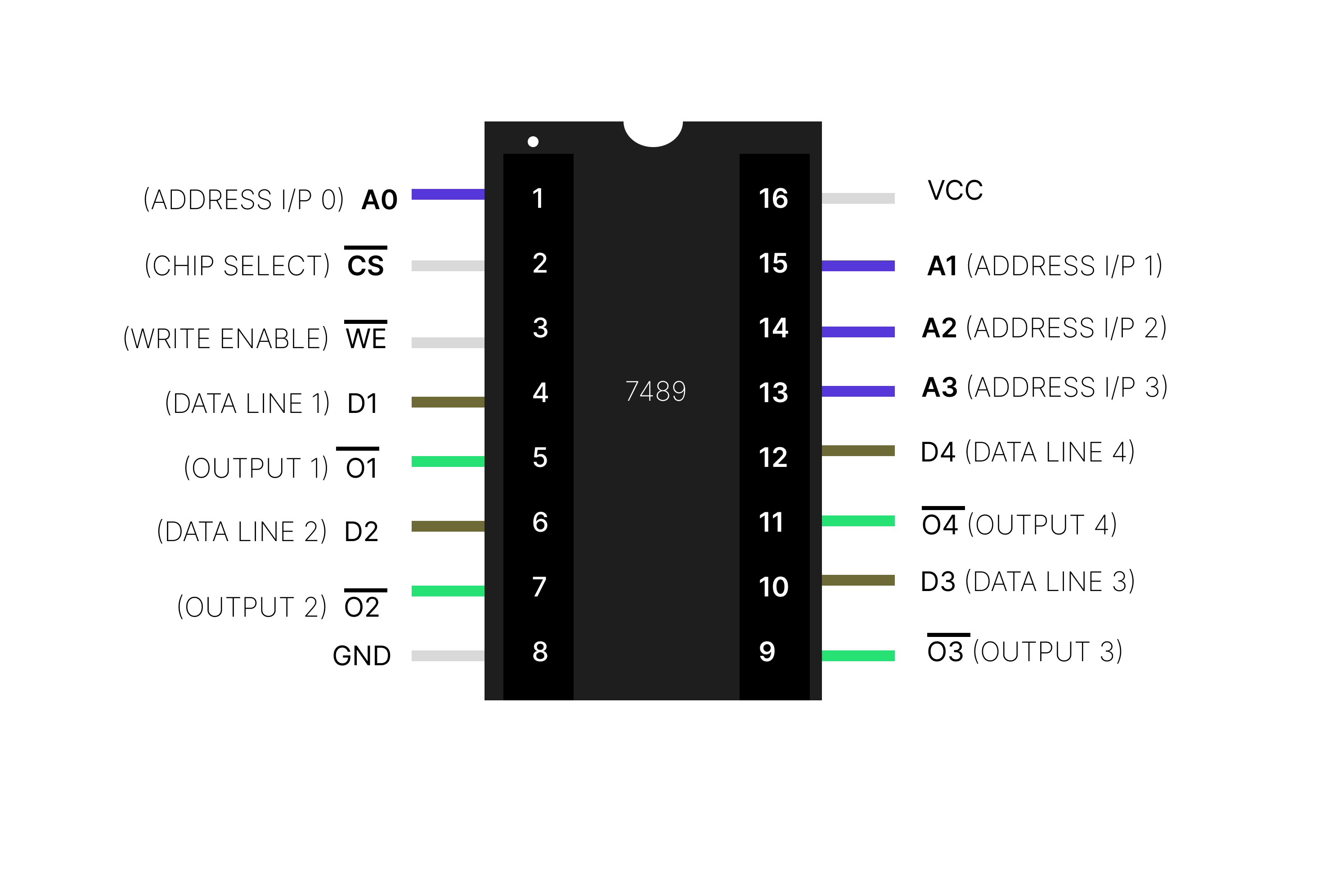
(7489 pinout )
The signals indicated here WE (Write Enable), CS (Chip Select), and O1, O2, O3, O4,represent active-low logic, meaning they are active when connected to logic level 0. Additionally, please note that the output comes from a RAM, and the value stored at the given address is reflected on the output in inverted form. By passing the output through a NOT gate (inverter), the original, non-inverted data can be retrieved. Please make a note of this.
Key Differences Between 74189 / 74219 and 7489 ICs
1. Open-Collector Outputs
The 7489 has open-collector outputs, where as 74189 or 74LS189 have tri-state outputsLets understand both these setups2. Tri-state output
Tri-state outputs (also called three-state logic) refer to digital output pins that can exist in three different states:
1.HIGH (1) : Output is actively driving a high voltage (usually 5V or 3.3V).
2.LOW (0) : Output is actively driving a low voltage (0V).
3.High Impedance: Output is disconnected from the circuit, like an open switch.
In short
It can drive both high and low logic levels.
Can also be disabled into a high-impedance (Hi-Z) state using an output enable pin.
No need for external pull-up resistors.
Below i given a pictire so that you can understand it easily
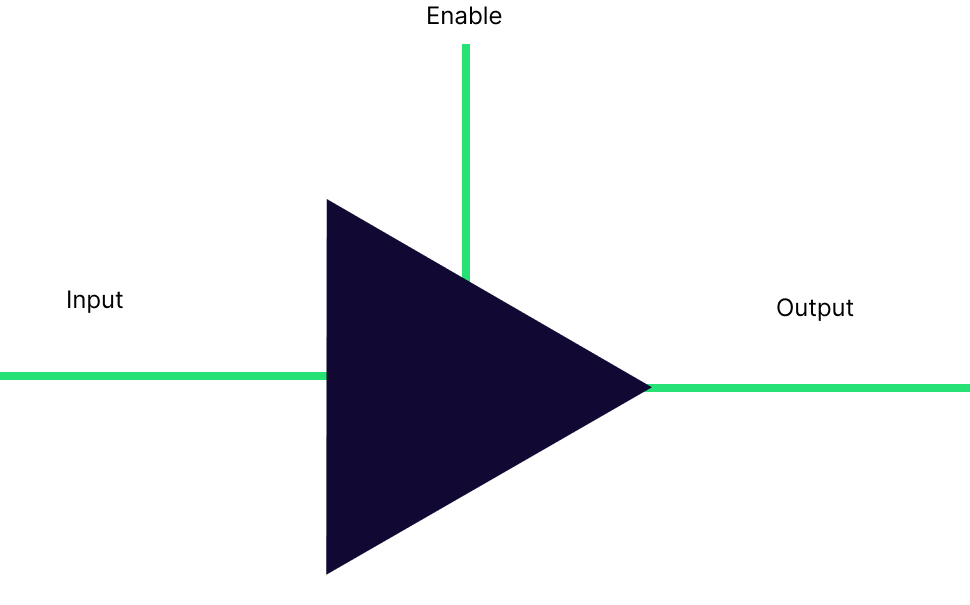
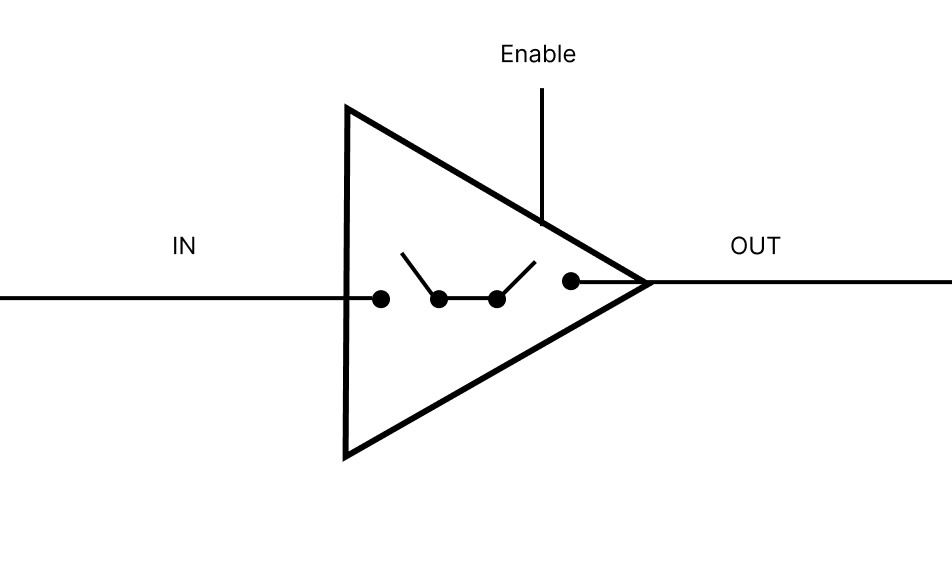
That is, when the enable signal is connected, the gate becomes active and its output depends on the input either high or low. If the enable signal is not present, the gate remains inactive and does not produce any output.
The enable signal can be either active-low or active-high, depending on the specific device. This means that, in some cases, the gate is activated by connecting the enable pin to a low logic level (active-low), while in others, it is activated by a high logic level (active-high). The exact behavior depends on the manufacturer's design, so it's important to check the datasheet to understand how the enable signal should be used.
2. Tri-state output
Tri-state outputs (also called three-state logic) refer to digital output pins that can exist in three different states:
1.HIGH (1) : Output is actively driving a high voltage (usually 5V or 3.3V).
2.LOW (0) : Output is actively driving a low voltage (0V).
3.High Impedance: Output is disconnected from the circuit, like an open switch.
In short
It can drive both high and low logic levels.
Can also be disabled into a high-impedance (Hi-Z) state using an output enable pin.
No need for external pull-up resistors.
Below i given a pictire so that you can understand it easily
That is, when the enable signal is connected, the gate becomes active and its output depends on the input either high or low. If the enable signal is not present, the gate remains inactive and does not produce any output.
The enable signal can be either active-low or active-high, depending on the specific device. This means that, in some cases, the gate is activated by connecting the enable pin to a low logic level (active-low), while in others, it is activated by a high logic level (active-high). The exact behavior depends on the manufacturer's design, so it's important to check the datasheet to understand how the enable signal should be used.
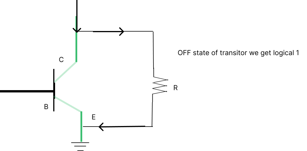
Open collector mechanism
An open collector (or open drain) output cannot actively drive a high logic level.
It can only pull the output low or leave it floating (disconnected).
A pull-up resistor is required to bring the line high when the output is inactive.
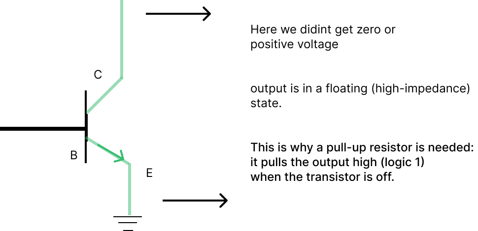
Look at the diagram to understand better
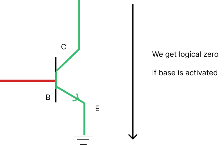
Explanantion summaryWhen base voltage is applied (transistor ON):
The transistor conducts
This connects the collector to ground, effectively pulling the output low (logic 0).
It's like "closing a switch" to ground.
When base voltage is NOT applied (transistor OFF):
The transistor is not conducting
The collector is disconnected — meaning the output is in a floating (high-impedance) state.
With base voltage → transistor ON → output pulled LOW (connected to GND)
No base voltage → transistor OFF → output FLOATING (open collector)
This is why a pull-up resistor is needed: it pulls the output high (logic 1) when the transistor is off.
When we use pull up resitor we get the outputs correctly
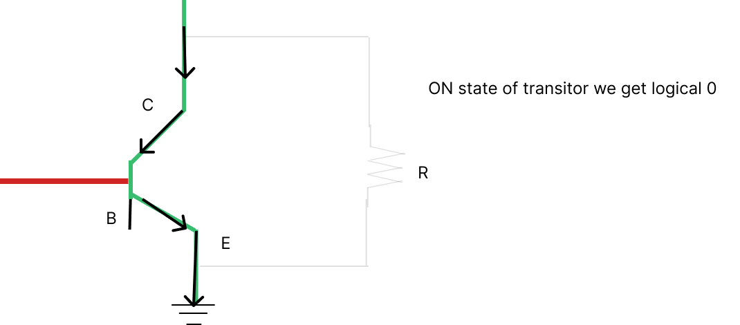
When base voltage is applied (transistor ON):
The transistor conducts
This connects the collector to ground, effectively pulling the output low (logic 0).
It's like "closing a switch" to ground.
When base voltage is NOT applied (transistor OFF):
The transistor is not conducting
The collector is disconnected — meaning the output is in a floating (high-impedance) state.
With base voltage → transistor ON → output pulled LOW (connected to GND)
No base voltage → transistor OFF → output FLOATING (open collector)
This is why a pull-up resistor is needed: it pulls the output high (logic 1) when the transistor is off.
When we use pull up resitor we get the outputs correctly
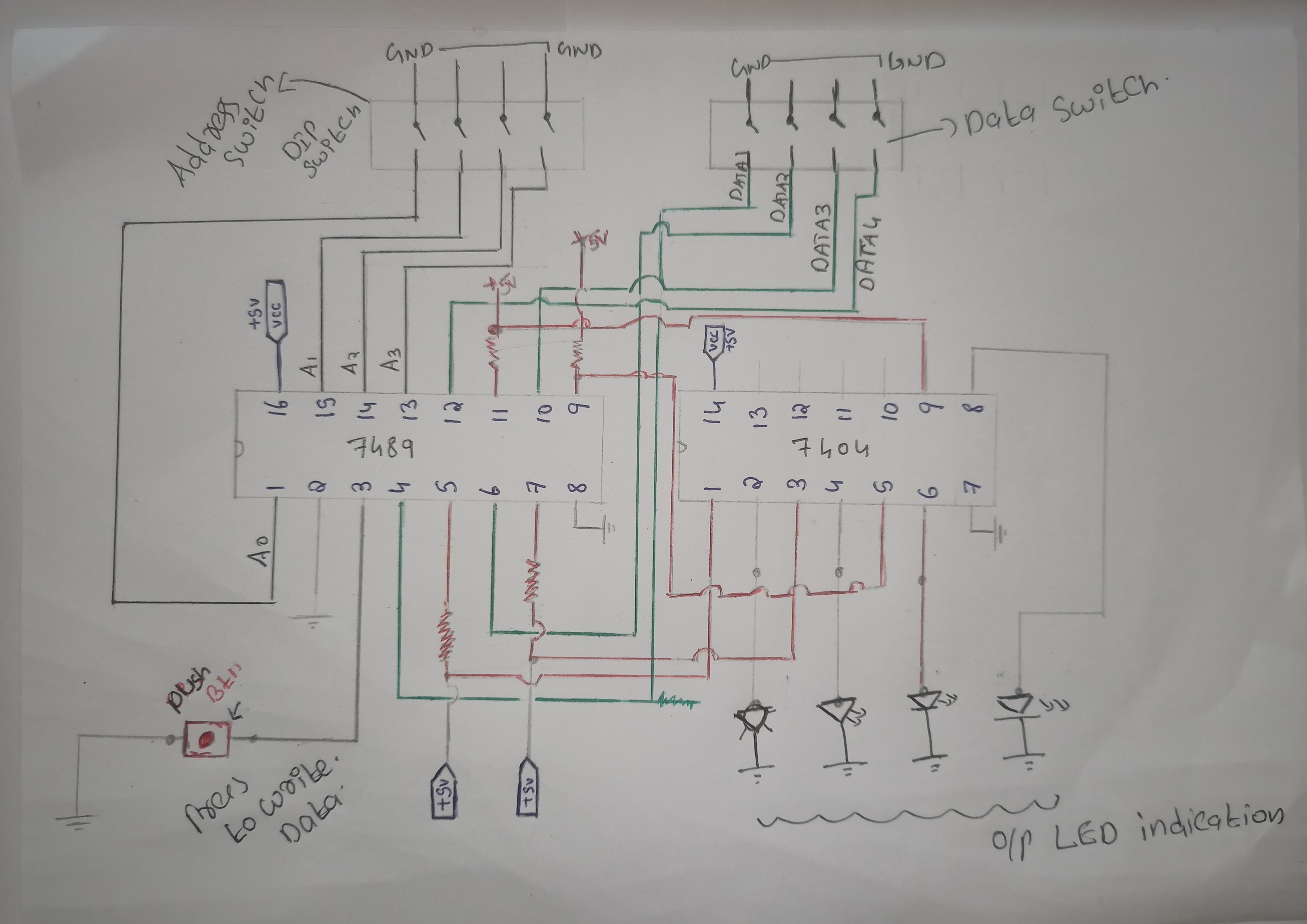
I think you've got the concept — so let's dive in and start building the RAM mechanism using DIP switches, LEDs, and other components. Let's go!
Hands-On RAM Controller: Address and Data Setup via DIP Switches with Manual Write Trigger
Circuit diagram